Radiation tolerance, power efficiency, and fast write performance also characterize F-RAM non-volatile storage technology. Home
Ferroelectric Random Access Memory (F-RAM) is a non-volatile storage technology that offers low power, fast write performance, and a greater write endurance when compared to EEPROM or flash technologies. For example, the write endurance of F-RAM from Cypress Semiconductor is 10^14 (100 trillion) write cycles. Presuming the device takes 4 ms to rewrite every cell, it would take a minimum of 126 years for a failure to occur. However, EEPROM and NOR Flash have write endurance of just 10^6 (1 million) write cycles. Additionally, F-RAM data retention is very robust, supporting a minimum of 10 years, and more than 121 years of data retention at + 85 °Cdeg;C, depending on the individual product.
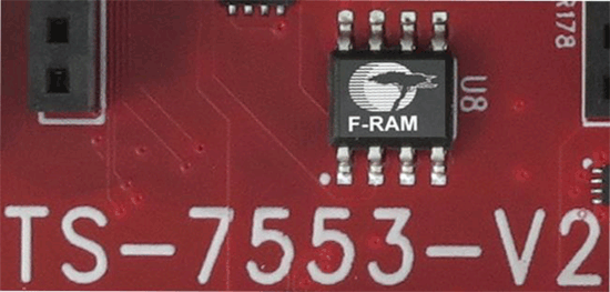
The high-speed nature of the device combined with its non-volatility and data retention makes this memory device useful in many applications. The F-RAM used in Technologic Systems’ products is an AT25 compatible SPI device. The TS-7553-V2 board support package implements the F-RAM as an extra EEPROM-like memory and presents the whole device as a flat file.
Use Cases for F-RAM
Attached as a simple memory device, F-RAM can be used to store any data an application may need to retain in either traditional RAM or non-volatile memory. Having a secondary memory device can be useful for applications such as per-unit configuration/calibration data, non-secure storage of unique serial numbers or IDs, and boot flags. Applications that can take advantage of the high write endurance of F-RAM memory include temporary storage that needs to remain non-volatile, counters that require frequent writes, or data logging applications that need to store local data logs that will be read or transmitted later.
F-RAM has also proven to be highly tolerant to radiation effects that may be experienced in airborne and space applications. Typical memories retain state using various techniques that are susceptible to corruption from alpha particles, cosmic rays, heavy ions, and gamma- and x-rays. For instance, Dynamic Random Access Memory (DRAM) stores charge in a capacitor. Static Random Access Memory (SRAM) sets a latch. And EEPROM typically stores charge in an insulated floating gate. Each of these can experience a bit-flip, or soft error, as a result of a radiation event. Because the F-RAM cell stores the state as a lead zirconate titanate (PZT) polarization, an alpha particle or heavy ion hit is very unlikely to cause the polarization to change a given cell’s state, resulting in a robust tolerance to these events.
As the number of high altitude and low earth orbit projects continues to grow, especially for small-sat/cube-sat style projects, single board computers will rely on serial I/O boot code and data logging memories. F-RAM is the robust choice for these harsh environments.
Construction and Operation
The ferroelectric in F-RAM refers to a type of crystal material that is made of tiny electric dipoles where the positive and negative charges have a slight separation. This electric polarization is a natural spontaneous state of particular types of crystals and can be controlled via the application of an external electric field. The ferroelectric property is a phenomenon observed in a class of materials such as the PZT used in Cypress’ F-RAM (Figure 2).
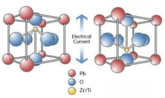
Applying an electric field across the crystal causes the position to be aligned in the direction of the field and, conversely, when the electric field is reversed the crystal will be aligned in the opposite position. The polarization will remain in its last state until an electric field is applied, allowing reliable, non-volatile memory to be constructed from these crystals.
F-RAM Operation
FRAM is constructed of ferroelectric crystals used as a capacitor dielectric in a structure similar to DRAM. Where flash or EEPROM technologies rely on a charge being trapped on a floating gate, DRAM captures its charge in a capacitor. The capacitor in the FRAM cell uses a ferroelectric material, typically lead zirconate titanate, as the dielectric. By using a ferroelectric polarized dielectric, the cell is able to maintain its current state without the constant charge current required by DRAM, and the state is able to persist even without power. Home
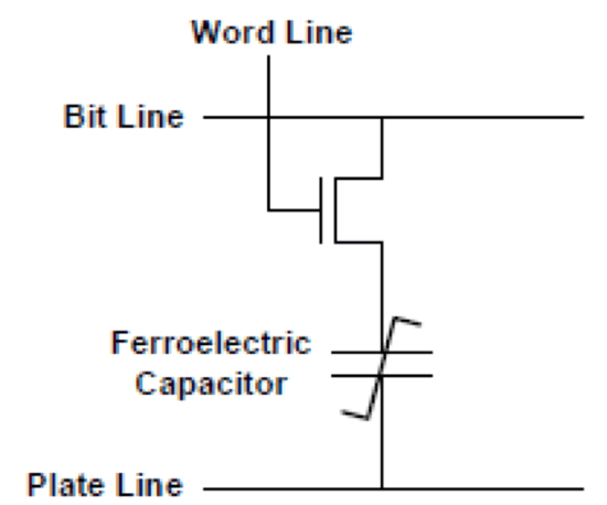
The ferroelectric capacitor symbol (Figure 3) indicates that the capacitance is variable and is not a traditional linear capacitor. If a ferroelectric capacitor is not switched when an electric field is applied (no change in polarization state), it behaves like a linear capacitor. If it is switched, there is an additional charge induced, therefore, the capacitance must increase. The ferroelectric capacitor is combined with an access transistor, a bit line, and a plate line to form the memory cell as shown in Figure 3.
The operation of an F-RAM cell is also similar to DRAM. Writing is accomplished by applying a field across the ferroelectric layer in the capacitor by charging the plates on either side of it. The direction of the charge orients the dipoles in the ferroelectric layer one way or the other. This is how logical “0” and “1” are represented.
A read operation is destructive to both DRAM and F-RAM. This means that after a read a rewrite must occur for the data to remain in the cell. In a DRAM read, the cell is drained to a sense amplifier. Next, it is determined if the cell contained a charge or not.
F-RAM is read by setting the cell to a known logical state, for example a “0.” If the cell is already in this state, then the output from the cell shows no change, and it is known that the cell was in a “0” state. However, if the cell is in the opposite state, the output from the cell is a brief current pulse as electrons are pushed out during the ferroelectric polarity switch. The internal controller will then reset the cell to the correct value to be stored back, and the read data is transferred out of the IC.

F-RAM Benefits Over Other Non-Volatile Memory
Traditional writable non-volatile memories that use floating gate technology such as EEPROM or Flash use charge pumps to develop high voltages on-chip (10 V or more) thus forcing carriers through the gate oxide. With charge pumps there are long write delays and high power consumption for write or erase operations. Additionally, the write operation is destructive to the memory cell, which limits the operating life. F-RAM’s crystalline structure does not have this sort of wear out mechanism from forcing carriers through oxides, ensuring a longer operating life. Also, the switching speed of the F-RAM’s crystalline structure supports an “instant write,” guaranteeing that when data is presented to the device the data is stored without any internal chip delay. This eliminates “data at risk” in case of a sudden power loss. The mechanism used to apply an electric field to the F-RAM structure also requires significantly less power than the power used by the charge pumps in floating gate technologies.
By Kris Bahnsen and Eliza Schaub, Technologic Systems Home
Originally published on eecatalog.com:
http://eecatalog.com/storage/2018/08/29/write-endurance-to-write-home-about/