Single Level Cell (SLC) NAND flash is no longer the stuff of headlines. Consumer markets are chasing the latest nodes and densities in Multi Level Cell (MLC), Tri-Level Cell (TLC), or the up and coming 3D NAND memories, leaving SLC NAND to the smaller “high reliability” market. However, in the world of embedded systems where product life cycles are measured in decades rather than years, SLC NAND is still in heavy use. Despite continued use in applications requiring long life or high-reliability solutions, NAND manufacturers have quietly made changes to their SLC NAND offerings that have slowly decreased the endurance of SLC NAND. Home
A Completely Different Story
The SLC NAND being manufactured today is not the same as the SLC NAND that was available even a few years ago. While today’s SLC NAND still has higher endurance than any other NAND technologies manufactured today, the endurance is significantly less than the 5x nm and larger SLC NAND of yesteryear. The 5x nm and larger SLC NAND devices need very little management to be reliable in an embedded system. Simple single bit error correcting algorithms more than suffice to make 5x nm and larger SLC NAND useable in most applications. A little bit of management and redundancy can make an embedded system with this NAND practically impervious to flash wear out, and even industry experts view wear-leveling as a “plus” in 5x nm SLC applications. Today’s SLC NAND devices, however, are a completely different story, and the industry has downplayed or overlooked the changes to SLC NAND in favor of its flashier cousins.
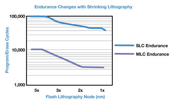
Along with DDR RAM, NAND flash has been a driver of lithographic process node scaling. When NAND was introduced in 1984, the size of the process node was 0.7μm and endurance was 100,000 or more program/erase cycles. This endurance was maintained through the 5x nm process nodes, but as it transitioned to 4x/3x nm technology, the endurance dropped to 70,000 and fewer program/erase cycles per cell (Figure 1). Current leading NAND lithographies are less than 2x nm. A closer look at NAND flash technology shows that even users of SLC NAND need to be concerned about decreasing NAND endurance, especially in embedded or high reliability applications.
The number of program/erase cycles a cell can endure before the erased state of cell is no longer discernible from the programmed state determines NAND flash endurance. However, in practical application it is determined by how long a flash cell can be used before unrecoverable data corruption occurs. There are several methods of data corruption, all of which are impacted by shrinking process lithographies. Home
Flash Memory Construction
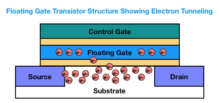
A single bit of flash memory is constructed of a transistor with a floating gate. The floating gate can be used to store electrons for an extended time. Electrons get to the floating gate by tunneling through to the thin oxide layer that isolates the floating gate (Figure 2). This tunneling effect is created when a large gate voltage is applied to the device. The gate voltage creates a field in the channel, increasing the energy of the electrons and causing some of them to tunnel through the thin oxide layer. The charge can be removed from the floating gate by reversing the gate voltage and pushing the electrons back through the thin oxide layer.
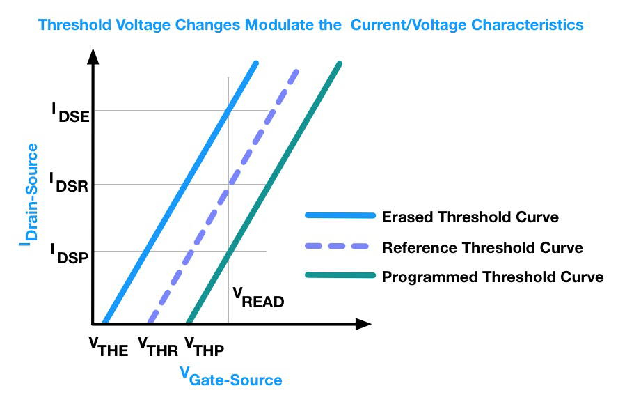
When electrons are stored on the floating gate, the threshold voltage, or the gate voltage where the transistor begins to conduct, changes. If there are no electrons on the gate, then the transistor acts like a normal MOSFET. When electrons are stored on the floating gate, their negative charge shields the conductive channel from the gate and prevents or limits the current flow from the source to the drain. This change in the threshold voltage modulates the current/voltage characteristics of the cell, so the status of the floating gate can be read by simply applying a voltage to the terminals and measuring the resulting current. Home
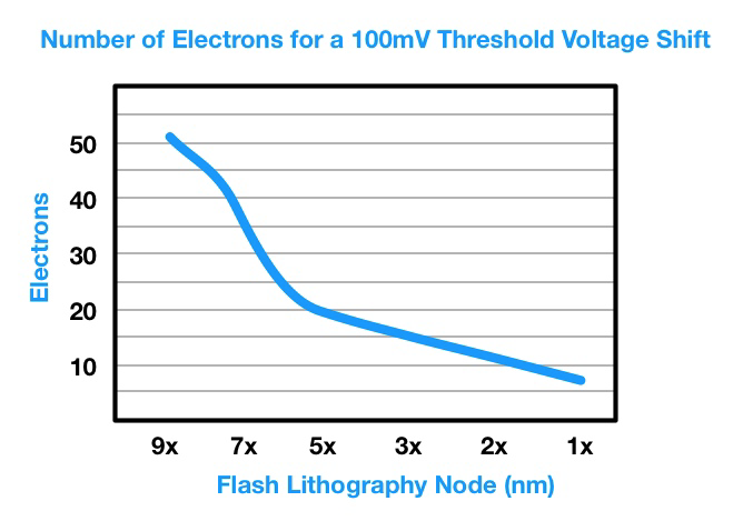
As the NAND flash lithography nodes are scaled down, the number of electrons available to move to the floating gate decreases. This is a well discussed fact for MLC NAND, but the same physics applies directly to SLC flash as well. In smaller lithographies, a small change in the number of electrons on the floating gate can dramatically affect the threshold voltage (Figure 3). With each reduction in NAND flash lithography, it becomes very difficult to achieve the same performance and endurance of the previous process node. The reduced number of electrons available makes smaller lithography devices even more susceptible to threshold voltage shifts caused by damage, leakage or disruptions.
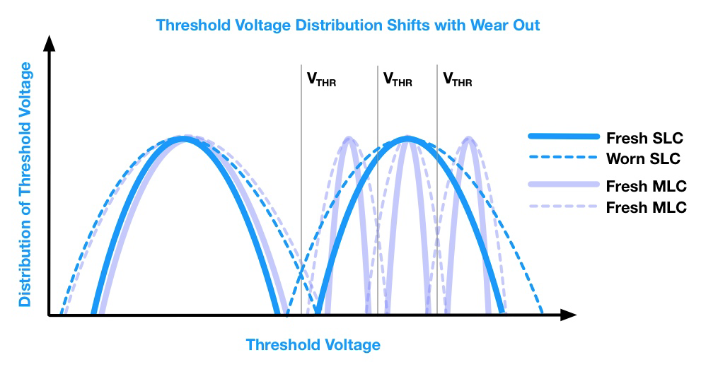
The gate threshold voltage is variable regardless of what lithography a NAND cell is made on. As it can be affected by a number of factors, it is typically expressed as a statistical distribution. The statistical distribution of the threshold voltage on new flash defines the difference between a programmed and an erased cell. The voltages used in programing a NAND flash cell slowly damage the thin oxide layer that isolates the floating gate, allowing more charge to be trapped on the floating gate. At any geometry, this damage will accumulate over time, narrowing the gap between the threshold regions and pushing the threshold voltage of an erased cell over the detection threshold used to detect the programmed state (Figures 4, 5). At smaller lithographies the geometries used in the NAND construction are even smaller, resulting in faster wear out and lower endurance. In an embedded system this means that the same software application can wear out newer SLC NAND at much faster rates than ever before.
Another source of variability in the gate threshold voltage is accidental charge collection. Flash cells are structured in vast arrays, with each cell packed tightly with its neighbors. Programming or reading a cell will apply elevated voltage stress to all the neighboring cells. Occasionally this stress will cause electrons to accidentally tunnel up onto the floating gates of the neighbor cells. As any change in charge will affect the threshold voltage of a cell, these accidental electrons can cause a cell to appear programmed when it should be erased. Luckily the acquisition of accidental electrons does not wear out the oxide layer, and the electrons are easily removed with an erase of the flash. With shrinking lithographies bringing individual cells closer to each other, the chances of accidental charge collection are much higher. Home
Error Correcting Techniques
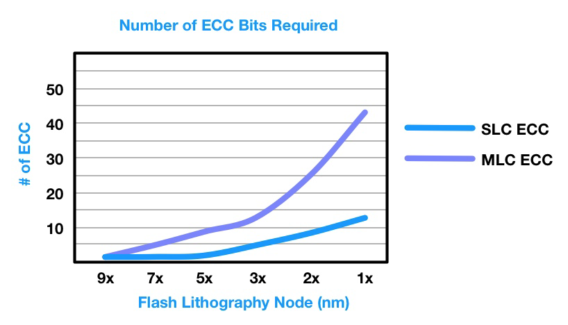
Accidental charge collection from a neighboring NAND cell being programed or read can be detected by using error correcting techniques. There are several error correction algorithms used with NAND flash, but all of them entail calculating and storing an extra value that allows an error to be detected, known as the Error Correcting Code (ECC). By utilizing the error correction algorithm as data is read back from the NAND flash, program or read disruptions in NAND cells can be detected. In addition to detecting the error, a small enough error can also be corrected. If the error is correctable, the affected NAND cell can be erased and reprogrammed again with the correct data and remain useful in an embedded system for many more program/erase cycles. Smaller lithography devices require more bits of ECC in order to compensate for the increased likelihood of a disruption due to the smaller geometries (Figure 6). A higher number of ECC bits required for a NAND flash device is frequently the best indicator that a smaller lithography is in use, and that the overall endurance of the device has also decreased.
SLC NAND manufacturers have been quietly rolling out smaller lithography devices with little comment about the decreasing endurance of the devices. SLC NAND flash users are being forced to transition to smaller lithography NAND flash as larger lithography devices are no longer available on the market. Embedded systems’ need for high reliability storage hasn’t changed, but suddenly the endurance of the SLC NAND has. The days of inherently reliable SLC NAND have silently slipped away leaving many embedded systems stuck with NAND flash that no longer endures under the same real life applications. How will the market adjust to address the needs of the end customers? Technologic Systems will be addressing it in its products by offering a state of the art SLC NAND management solution. For details about this new NAND management layer please read our white paper “XNAND2: NAND Device Driver for Today’s Lower Endurance SLC NAND”. Home
References:
- “Advanced Flash Technology Status, Scaling Trends & Implications to Enterprise Scaling Trends & Implications to Enterprise SSD Technology” by Jung H. Yoon & Gary A. Tressler, IBM Corporation, Aug 21, 2012
- Cypress Semiconductor “AN200602 SLC Versus MLC NAND Flash Memory” Document No. 002-00602 Rev. *A, Nov 6, 2015
- “The Inconvenient Truths of NAND Flash Memory” by Jim Cooke, Micron Technology, Aug 2007
- “Modelling of the threshold voltage distributions of sub-20nm NAND flash memory” by T. Parnell, N. Papandreou, T. Mittelholzer, H. Pozidis, IBM Research — Zurich, Switzerland, March 2015
- Santa Clara University,COEN 180“Floating Gate Basics” by Thomas Schwarz, 2003
- “Nonvolatile Memories: NOR vs. NAND Architectures” by L. Crippa, R. Micheloni, I. Motta and M. Sangalli, Qimonda Design Center & Numonyx, 2008
- New Electronics Digital Magazine “No FLASH in the pan” by Axel Stoermann, Toshiba, Oct. 14, 2014
- Cactus Technologies, “SLC vs MLC and The Impact of Technology Scaling”
One thought on “SLC NAND: Secrets Exposed”